Dissertation
by
Andy Revenko
—
last modified
Jul 27, 2009 11:40 AM
Dissertation page
Education
1999 – 2001 – engineer, chair of informatics in Berdyansk State Pedagogical University
2002 – 2008 - senior teacher, chairs of informatics and physics at Berdyansk State Pedagogical University
2009 – research officer, chair Semiconductors Electronics, Laboratory of Automation of Scientific Investigation, Kiev National University
Kidalov V.V., Sukach G. A., Revenko A.S., Bayda A.D., Properties of cubic GaN films obtained by nitridation of porous GaAs (001) // Phys. Stat. Sol. (a). - 2005. - Vol. 202, № 8. - P. 1668-1672.
Kidalov V.V., Sukach G.A., Revenko A.S., Potapenko E.P., Photoluminescent and structural properties of GaN thin films obtained by radical - beam hettering epitaxy on porous GaAs(001) // J. Lumin. - 2003.- Vol. 102-103. - P. 712-714.
Vlasenko N.A., Kotljarevsky M.B., Kidalov V.V., Denisova Z. L., Kononets Ya. F., Revenko A.S., Veligura L.I. Effect of Co-Doping with Oxygen on the Characteristics of ZnS:Mn Thin-Film Electroluminescent Structures // Phys. stat. sol. (a). – 2002. – Vol.193, № 2. – P. 338 – 346.
V.V. Kidalov, G.A.Sukach, A.S. Revenko and E. P. Potapenko “Ultraviolet luminescence of thin GaN films grown by radical-beam gettering epitaxy on porous GaAs(111) substrates”, Semiconductors, 2003, Vol. 37, Number 11, pp. 1264-1265.
M.B. Kotlyarevskii , G.A. Sukach, V.V. Kidalov and A. S. Revenko “Luminescence of GaN Layers Grown on GaAs Substrates by the Method of Radical-Beam Epitaxy”, Journal of Applied Spectroscopy, 2000,Vol. 69, Number 2, pp. 270-274.
Kidalov V.V., Sukach G.A., Revenko A.S., Model of the nitridation process of nanoporous GaAs surface // The fifth international conference on low dimensional structures and devise (12 - 17 December, 2004). - Cancyne Maiyna Riviera Mexico, 2004. - P. 368 – 369.
Kidalov V.V.,Revenko A.S., Simulation of Diffusion Process at Nitridation of GaAs substrate // 2007 Fall Meeting of Electrochemical society of Japan (ECSJ) - Section - Organic & biological Electrochemistry (May 15 - 20, 2005). - Guebec city, Canada, 2005. - Abs. №1405
Kidalov V.V., Sukach G.A., Beji L., Revenko A. S., Bayda A.D., Properties of Porous GaAs Substrate for III-N Epitaxy // 2008 Fall Meeting of Electrochemical society of Japan (ECSJ) Section L1 - Nitride and Wide Bandgap Semiconductors for Sensors, Photonics, and Electronics VI ( 16 - 21 October, 2005 p.). - Los Angeles, California, USA, Abs. №808.
Kidalov V.V., Beji L., Suckach G. A., Revenko A.S., Bayda A.D., Yatsenko Y., Raman spectroscopy and morphology investigation of porous GaAs // E-MRS Fall meeting. Section Interfacial processes and properties of advanced materials (5-9 September, 2005). - Warsaw, Poland, 2005. - P. 145.
- Berdyansk State Pedagogical University, faculty of physics and mathematics (1993-98), Diploma with Honor.
- Postgraduate at Zaporizhzhya National University (2001-2004), specialty – “physics of semiconductors.”
Scientific Degree Ph. D. in Physics, 2007 (defending a thesis was hold in National Taras Shevchenko University of Kyiv).
Theme of Ph.D thesis “Properties of GaN films, obtained by nitridation of porous GaAs substrate”
Researching activities is devoted to:
- Mathematic simulation of atoms interaction during diffusion process and convertation one material into another (GaAs surface layer into GaN thin films) during annealing of substrates in nitrogen plasma.
- Improving technology of obtaining nonexpensive and quality GaN/porous-GaAs structure as substrate material for epitaxial growth of strain-free GaN films. Reducing mechanical strain in interface of GaN/GaAs structure with the help of using porous GaAs substrate allow to improve structural, optical and electrical properties of GaN films.
- Investigation the dependences of structural, morphology and optical properties of different materials (GaN, GaN, GaNAs, ZnS) on technological parameters of treatments in nitrogen plasma and properties of substrates.
 |
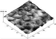 |
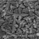
| Porous GaAs substrate | GaN films on porous GaAs substrate |
 |
 |
 |
|
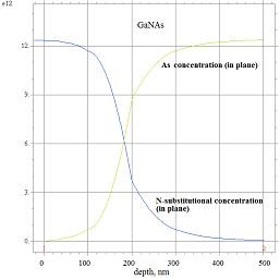
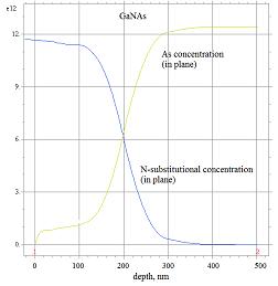
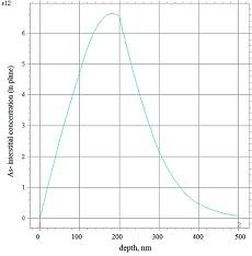
| Concentration profile of substitutional Nitrogen and Arsenic atoms in GaN/GaAs structure | Concentration profile of substitutional Nitrogen and Arsenic atoms in ternary compound GaNAs | Concentration profile of interstitial atoms of As in ternary GaNAs compound | |
| Results were obtained by numeric solving of the system of coupled diffusional-interaction differential equations Solving and analyze of mathematic model were processing in mathematical packages Maple and FlexPDe |
|
||
Works
Research position
1998-2005 - Senior research at laboratory “Physics of optoelectronics” (at Berdyansk State pedagogical University) within framework of performing following State Funded Project (supported by Ministry of Science and Education of Ukraine) :
- “Technology of radical-beam epitaxy of hetero-structures on the base of A3B5 compounds”.
- “Radical-beam hettering epitaxy as a new method in technology of semiconductors devices structures on the base of multy-component A3B3 compound”.
- “Ultraviolet lasers on the base of nano-porous GaAs”
2006-2007 – Senior research at the Institute of Nanotechnologies and System Engineering (at Berdyansk State Pedagogical University).
Teaching position (combine jobs)Pincipal publications
Some Conferences
